| VCC max | ±37 | V. |
| VCC | ±24.5 | V. |
| RL | 8 | ohm |
| PO (1) | 20 | W. |
| fL, fH | 20 to 50k | Hz |
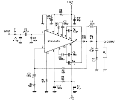
Description of External Parts
R1, C1 : Input filter circuit
• Reduces high-frequency noise.
C2 : Input coupling capacitor
• DC current suppression. A reduction in reactance is effective because of increases in capacitor
reactance at low frequencies and 1/f noise dependence on signal source resistance which result in
output noise worsening.
R2 : Input bias resistor
• Biases the input pin to zero.
• Effects VN stability (refer to NF circuit).
• Due to differential input, input resistance is more or less determined by this resistance value.
R4, R5,C3 (R2) : NFB circuit (AC NF circuit). Use of resistor with 1% error is suggested.
R3 : Differential constant-current bias resistor
R6, R7 : For oscillation suppression and phase compensation applications (For use with differential stage applications)
R7, C4 : For oscillation suppression and phase compensation applications (A Mylar capacitor is recommended for C4 for use with output stage applications)
C6, C9 : For oscillation suppression and phase compensation applicationsPower stage (Must be connected near the pin) C6: Positive (+) power C9: Negative (–) power
C8 : For oscillation suppression and phase compensation applications (Oscillation suppression before power step clip)
C5 : For oscillation suppression and distortion improvement applications
R8, C10 : Ripple filter circuit on positive (+) side.
R9, C13 : Ripple filter circuit on negative (–) side.
C11, C12 : For oscillation suppression applications
• Used for reducing power supply impedance to stable IC operation and should be connected near the IC
pin. We recommend that you use an electrolytic capacitor.
POWER SUPPLY FOR STK402V 20W. AF PA CIRCUIT
PRINTED CIRCUIT PATTERN FOR 20W. STK402V AF PA CIRCUIT


