Thursday, October 22, 2009

TPA2013D1 2.7-W CONSTANT OUTPUT POWER CLASS-D AUDIO AMPLIFIER CIRCUIT


image The TPA2013D1 is a high efficiency Class-D audio power amplifier with an integrated boost converter. It drives up to 2.7 W (10% THD+N) into a 4 Ω speaker. With 85% typical efficiency, the TPA2013D1 helps extend battery life when playing audio. The built-in boost converter generates the voltage rail for the Class-D amplifier. This provides a louder audio output than a stand-alone amplifier connected directly to the battery. It also maintains a consistent loudness, regardless of battery voltage. Additionally the boost converter can be used to supply external devices. The TPA2013D1 has an integrated low pass filter to improve RF rejection and reduce out-of-band noise, increasing the signal to noise ratio (SNR). A built-in
PLL synchronizes the boost converter and Class-D
switching frequencies, thus eliminating beat
frequencies and improving audio quality. All outputs
are fully protected against shorts to ground, power
supply, and output-to-output shorts.
TPA2013D1 DATASHEET

Read more >>

LA47202P 47 W. 4 CH BTL Power Amplifier for Car Audio Systems

image

LA7202P 47W. 4CH BLOCK DIAGRAM

VCC max1 Without signal, t = 1 minute  26 V
VCC max2 When operating = 18 V
VCC = 14.4 V
RL = 4 Ω

The LA47202P is a 4-channel BTL power amplifier IC developed for use in car audio applications. The LA47202P adopts a pure complementary output stage circuit structure with a v-pnp transistor for the high side and an npn transistor for the low side to provide both high output power and high quality sound. The LA47202P integrates all the functions required for car audio applications on the same chip, including a standby switch, a muting function, and a full complement of protection circuits. It also features a self diagnostics function.
LA7202P DATASHEET

Read more >>

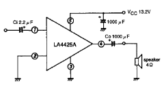
LA4425A 5W. POWER AMPLIFIER WITH VERY FEW EXTERNAL PARTS FOR CAR RADIO AND CAR STEREO CIRCUIT

circuit VCC max = 0 18 V
VCC = 13.2 V.
RL = 4 OHM
PO = 5 W.
fL =  40 Hz
fH = 90 kHz
Features

  • The world’s first power amplifier with very few external
    parts.
  • Almost no evaluation, adjustment and check of its functions
    as a power IC required
  • Wide operation supply range ® 5 to 16V
  • On-chip protection:
    Overvoltage protection
    Thermal protection
    Output D.C. short protection
  • On-chip pop noise reducing circuit

pcb

LA4425A 5W. Printed Circuit Pattern

LA4425A DATASHEET

Read more >>

Tuesday, October 20, 2009

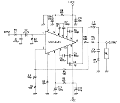
STK4171V 40W+40W AF POWER AMPLIFIER CIRCUIT

circuit

VCC max = ±49 V
VCC = ±32.5 V
RL =  8 ohm
PO = 40 W.
fL,fH = 20 to 50k  Hz

Description of External Parts

C3, C4

Input filter capacitors
• A filter formed with R5 or R6 can be used to reduce noise at high frequencies.

C5, C6

Input coupling capacitors
• Used to block DC current. When the reactance of the capacitor increases at low frequencies, the dependence of 1/f noise on signal source
resistance causes the output noise to worsen. It is better to decrease the reactance.
• To reduce the pop noise at the time of application of power, it is effective to increase C5, C6 that fix the time constant on the input side and
to decrease C9, C10 on the NF side.

C9, C10

NF capacitors
• These capacitors fix the low cutoff frequency

C19

Decoupling capacitor
• Used to eliminate the ripple components that mix into the input side from the power line (+VCC).

C15, C16

Bootstrap capacitors
• When the capacitor value is decreased, the distortion is liable to be higher at low frequencies.

C17, C18

Oscillation blocking capacitors
• Must be inserted as close to the IC power supply pins as possible so that the power supply impedance is decreased to operate the IC stably.
• Electrolytic capacitors are recommended for C17, C18.

C20

Capacitor for ripple filter
• Capacitor for the TR12-used ripple filter in the IC system

C13

Oscillation blocking capacitor
• A polyester film capacitor, being excellent in temperature characteristic, frequency characteristic, is recommended for C13.

R5, R6 Resistors for input filter
R3, R4

Input bias resistors
• Used to bias the input pin potential to zero. These resistors fix the input impedance practically.

R7, R9
(R8, R10)

These resistors fix voltage gain VG.
It is recommended to use R7 (R8) = 560 R9 (R10) = 56k for VG = 40dB.
• To adjust VG, it is desirable to change R7 (or R8).
• When R7 (or R8) is changed to adjust VG, R3 (=R4) =R9 (=R10) must be set to ensure VN balance.

R11, R20
(R12, R21)

Bootstrap resistors
• The quiescent current is set by these resistors 3.3k
+ 3.3k It is recommended to use this resistor value.

R15

Resistor for ripple filter
• (Limiting resistor for predriver TR at the time of load short)

R14 Used to ensure plus/minus balance at the time of clip.
R18, R19

Resistor for ripple filter
• When muting TR13 is turned ON, current flows from ground to -VCC through TR 13. It is recommended to use 1k (1W) + 1k (1W) allowing for the power that may be dissipated on that occasion.

R24, R25 Oscillation blocking resistors
R22, R23 Oscillation blocking resistors
L1, L2 Oscillation blocking coils

supply

POWER SUPPLY FOR STK4171V 40+40 W. AF PA CIRCUIT

ptinted

PRINTED CIRCUIT PATTERN FOR STK4171V 40+40 W. AF PA CIRCUIT

Read more >>

Monday, October 19, 2009

STK4102II 10W+10W AF POWER AMPLIFIER CIRCUIT

circuit

VCC = ±17 V
RL = 8 ohm
VCC = ±20.5V
Po = 10w.
fL, fH = 20 to 50k Hz

Description of External Parts
C1, C2 Input filter capacitors
• A filter formed with R3 or R4 can be used to reduce noise at high frequencies.
C3, C4 Input coupling capacitors
• Used to block DC current. When the reactance of the capacitor increases at low frequencies, the dependence of 1/f noise on signal sourceresistance causes the output noise to worsen. It is better to decrease the reactance.
• To reduce the pop noise at the time of application of power, it is effective to increase C3, C4 that fix the time constant on the input side and
to decrease C5, C6 on the NF side.
C5, C6 NF capacitors
• These capacitors fix the low cutoff frequency
C15 Decoupling capacitor
• Used to eliminate the ripple components that mix into the input side from the power line (+VCC).
C11, C12 Bootstrap capacitors
• When the capacitor value is decreased, the distortion is liable to be higher at low frequencies.
C9, C10 Oscillation blocking capacitors
• Must be inserted as close to the IC power supply pins as possible so that the power supply impedance is decreased to operate the IC stably.
• Electrolytic capacitors are recommended for C9, C10.
C14 Capacitor for ripple filter
• Capacitor for the TR10-used ripple filter in the IC system
C7 Oscillation blocking capacitor
• A polyester film capacitor, being excellent in temperature characteristic, frequency characteristic, is recommended for C7.
R3, R4 Resistors for input filter
R1, R2 Input bias resistors
• Used to bias the input pin potential to zero. These resistors fix the input impedance practically.

R5, R9 (R6, R10) These resistors fix voltage gain VG. It is recommended to use R5 (R6) = 560 , R9 (R10) = 56k for
VG = 40dB.
• To adjust VG, it is desirable to change R9 (or R10).
• When R9 (or R10) is changed to adjust VG, R1 (=R2) =R9 (=R10) must be set to ensure VN balance.
R11, R13 (R12, R14) Bootstrap resistors
• The quiescent current is set by these resistors
2.2k + 2.2k It is recommended to use this resistor value.
R21 Resistor for ripple filter
(Limiting resistor for predriver transistor at the time of load short)
R18 Used to ensure plus/minus balance at the time of clip.
R19, R20 Resistor for ripple filter
• When muting TR11 is turned ON, current flows from ground to -VCC through TR 11. It is recommended to use 1k (1/2) + 1k (1/2W) allowing for the power that may be dissipated on that occasion.
R15, R16 Oscillation blocking resistors
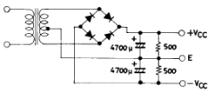
power-supply

POWER SUPPLY FOR STK4112II 210+10 W. AF AMPLIFIER CIRCUIT


printed

PRINTED CIRCUIT PATTERN FOR STK4112II 210+10 W. AF AMPLIFIER CIRCUIT

Read more >>

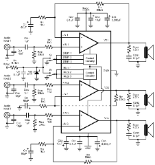
LM4734 3 CHANNEL 20W AUDIO POWER AMPLIFIER WITH MUTE AND STANDBY CIRCUIT

to-220

The LM4734 is a three channel audio amplifier capable of
typically delivering 20W per channel of continuous average
output power into a 4Ω or 8Ω load with less than 10%
THD+N from 20Hz - 20kHz.The LM4734 has short circuit protection and a thermal shut down feature that is activated when the die temperature exceeds 150°C. The LM4734 also has an under voltage lock
out feature for click and pop free power on and off.
Each amplifier of the LM4734 has an independent smooth
transition fade-in/out mute and a power conserving standby
mode. The mute and standby modes can be controlled by
external logic. The LM4734 has a wide supply operating supply range from±10V - ±30V allowing for lower cost unregulated power supplies to be used. The LM4734 can easily be configured for bridge or parallel operation for higher power and bi-amp solutions.

Key Specifications

  • Output Power/Channel with 10% THD+N,1kHz into 4Ω or 8Ω 20W (typ)
  • THD+N at 3x1W into 8Ω, 1kHz 0.03% (typ)
  • Mute Attenuation 110dB (typ)
  • PSRR 64dB (typ)
  • Slew Rate 18V/μs (typ)

Features

  • Low external component count
  • Quiet fade-in/out mute mode
  • Low power standby mode
  • Wide supply range: 20V – 60V

Applications

  • Audio amplifier for component stereo
  • Audio amplifier for compact stereo
  • Audio amplifier for home theater in a box (HTB)
  • Audio amplifier for high-end and HD TVs

pin Connection Diagrams LM4734

circuit

LM4734 20W. AF AMPLIFIER CIRCUIT DIAGRAM

laout

Composite Layer and  Silk Layer

pcb

Top Layer and Bottom Layer

Printed Circuit Pattern for Application Circuit

Read more >>

Saturday, October 17, 2009

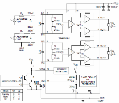
TDA8944J 2x7W STERIO BRIDGE TIED LOAD AUDIO AMPLIFIER CIRCUIT

circuit

General description
The TDA8944J is a dual-channel audio power amplifier with an output power of 2x7 W at an 8 W load and a 12 V supply. The circuit contains two Bridge Tied Load
(BTL) amplifiers with an all-NPN output stage and standby/mute logic. The TDA8944Jcomes in a 17-pin DIL-bent-SIL (DBS) power package. The TDA8944J is printed-circuit board (PCB) compatible with all other types in the TDA894x family.One PCB footprint accommodates both the mono and the stereo products.

Features

  • Few external components
  • Fixed gain
  • Standby and mute mode
  • No on/off switching plops
  • Low standby current
  • High supply voltage ripple rejection
  • Outputs short-circuit protected to ground, supply and across the load
  • Thermally protected
  • Printed-circuit board compatible

Applications

  • Mains fed applications (e.g. TV sound)
  • PC audio
  • Portable audio.
Symbol Parameter Conditions Min Typ Max Unit
Po output power

THD = 10%; RL = 8 W;
VCC = 12 V

6 7 - W
THD output power Po = 1 W - 0.03 0.1 %
Gv voltage gain   31 32 33 dB
SVRR

supply voltage ripple
rejection

  50 65 - dB
pin

 Pin description

Symbol

Pin

Description

OUT1- 1 negative loudspeaker terminal 1
GND1 2 ground channel 1
VCC1 3 supply voltage channel 1
OUT1+ 4 positive loudspeaker terminal 1
n.c. 5 not connected
IN1+ 6 positive input 1
n.c. 7 not connected
IN1- 8 negative input 1
IN2- 9 negative input 2
MODE 10 half supply voltage decoupling (ripple rejection)
SVR 11 half supply voltage decoupling (ripple rejection)
IN2+ 12 positive input 2
n.c. 13 not connected
OUT2- 14 negative loudspeaker terminal 2
GND2 15 ground channel 2
VCC2 16 supply voltage channel 2
OUT2+ 17 positive loudspeaker terminal 2

pcb

Printed-circuit board for TDA8944J

laout

Printed-circuit board layout for TDA8944J

Read more >>

STK402V 20W. AF POWER AMPLIFIER CIRCUIT

circuit 

VCC max ±37 V.
VCC ±24.5 V.
RL 8 ohm
PO (1) 20 W.
fL, fH 20 to 50k Hz

Description of External Parts
R1, C1 : Input filter circuit
• Reduces high-frequency noise.
C2 : Input coupling capacitor
• DC current suppression. A reduction in reactance is effective because of increases in capacitor
reactance at low frequencies and 1/f noise dependence on signal source resistance which result in
output noise worsening.
R2 : Input bias resistor
• Biases the input pin to zero.
• Effects VN stability (refer to NF circuit).
• Due to differential input, input resistance is more or less determined by this resistance value.
R4, R5,C3 (R2) : NFB circuit (AC NF circuit). Use of resistor with 1% error is suggested.
R3 : Differential constant-current bias resistor
R6, R7 : For oscillation suppression and phase compensation applications (For use with differential stage applications)
R7, C4 : For oscillation suppression and phase compensation applications (A Mylar capacitor is recommended for C4 for use with output stage applications)
C6, C9 : For oscillation suppression and phase compensation applicationsPower stage (Must be connected near the pin) C6: Positive (+) power C9: Negative (–) power
C8 : For oscillation suppression and phase compensation applications (Oscillation suppression before power step clip)
C5 : For oscillation suppression and distortion improvement applications
R8, C10 : Ripple filter circuit on positive (+) side.
R9, C13 : Ripple filter circuit on negative (–) side.
C11, C12 : For oscillation suppression applications
• Used for reducing power supply impedance to stable IC operation and should be connected near the IC
pin. We recommend that you use an electrolytic capacitor.
power-supply

POWER SUPPLY FOR STK402V 20W. AF PA CIRCUIT

printed-circuit

PRINTED CIRCUIT PATTERN FOR 20W. STK402V AF PA CIRCUIT

Read more >>

Features of the IMST Hybrid ICs

stk

1.  Excellent heat dissipation
    One of the most influential factors determining reliability of electronics devices is  “heat”
The IMST substrate is most suitable for the field of power electronics. Dissipating heat efficiently
2.  High  reliability
    Wiring is applied by mounting semiconductor bare ships directly and bonding aluminum wires. This reduces number of soldering points assuring high reliability.
3.  Excellent electromagnetic shielding
  Excellent electromagnetic shielding can be attained by putting the entire substrate on the ground potential because the  base substrate is made of aluminum. This eliminates noise errors in the digitalized electronic devices
4.  Ample lineup
    STK series lineup is ample and standard based whereas the current hybrid IC market tends to customization.
        Output power (per channel)    : 5 to  200W
        Total harmonic distortion        : 10 to 0.005%
        Number of channels            : 1 to 3ch
        Load impedance            : 1 to 8 Ohm
5. Pin compatibility
    The design takes pin compatibility of the hybrid IC output pin important so that a same PCB can be  used for various set grades such as output capacity and distortion factor.
6. Excellent thermal stability
    The IMST substrate of excellent heat dissipation naturally assures excellent thermal conductivity. Temperature of the output transistor can be almost the same as the temperature compensating transistor. Preventing thermal runway.
7. Decreasing adjustment processes
    Adjustment of the natural voltage of the power output stage and the quiescent current are done by functional trimming inside the hybrid IC.
This eliminates adjustment processes saving on the production procedure.
8.  Reducing the term for design
The audio output stage remains analog however digitalization technology may advance.
Design of the analog power output stage which is considered requiring the designer’s experience and skill, can be simplified by employing hybrid ICs.
This reduces the term for design and saves on the design procedure.
9.  Decreasing number of parts
    The product of STK series decreases the total number of parts required for a unit allowing to reduce its size, certain assembly manpower, simplify material control improve serviceability and reduce cost.
10. No smoke for fire
    Since the product of STK series is designed so to emit no smoke nor fire in any abnormality, it facilitates to obtain safety approvals.

Read more >>

IC AUDIO AMPLIFIER CUICUITS

stk-amp

Welcome to my ic-audio-amplifier-circuits blog.
Here you will learn about audio amplifier circuits with integrated circuit tips and how to find good information.

Read more >>